3 hours
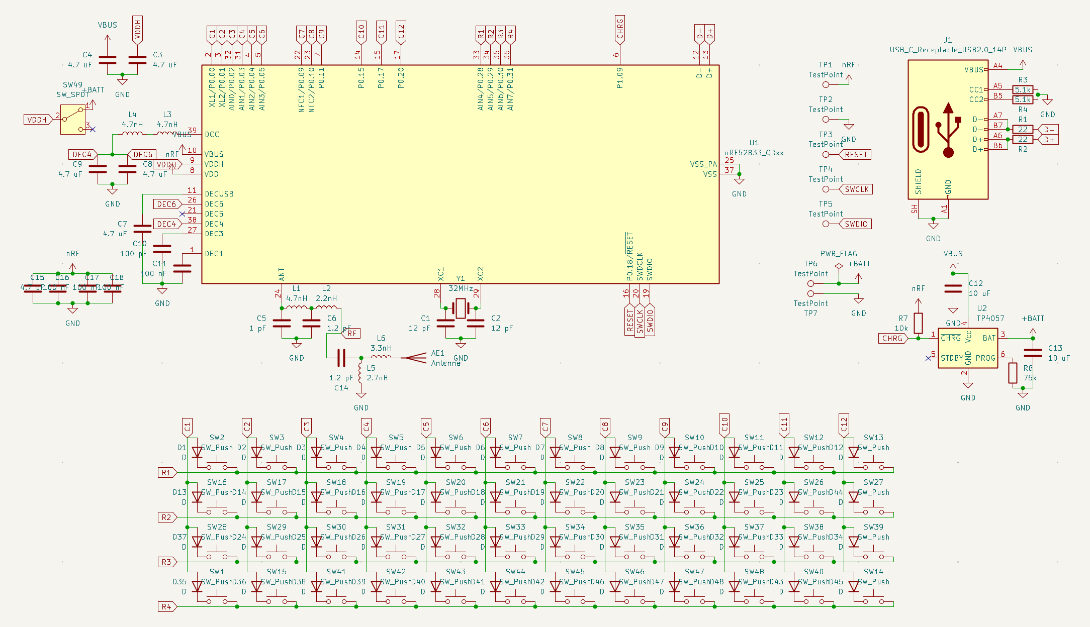
I designed the schematic for the keyboard.
Based on the datasheet, the nRF requires a surprising amount of extra caps and resistors to function, which are around the chip in the schematic. It took a while to figure out even how to exactly lay out the components, since the density of them is pretty high in certain areas.
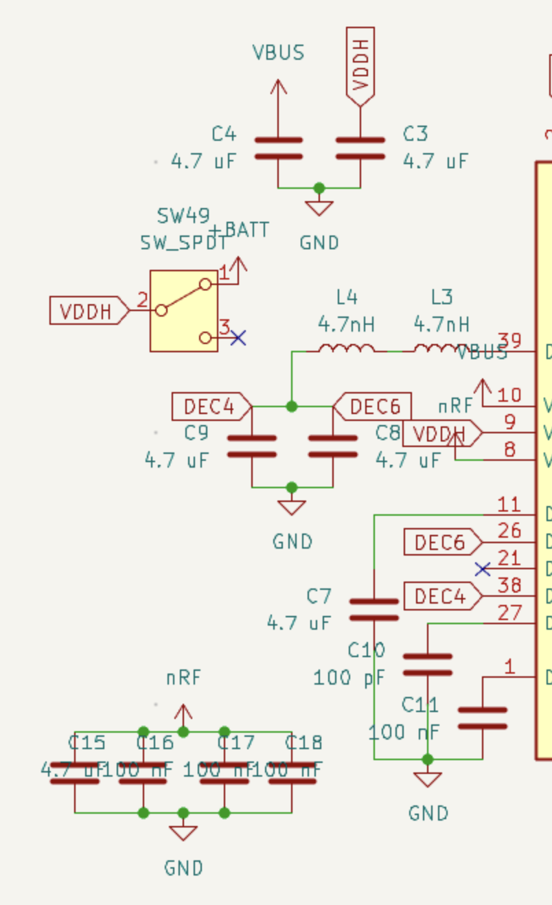
Also pictured there, I added a switch to toggle the chip’s connection to the battery. However, the battery still remains connected to the charger to allow for charging while the keyboard is off.
On the right side, there are some testpoints that function as pads for connecting the SWD pins (temporarily, for flashing the proper USB bootloader) and the LiPo battery.

The main challenge for the schematic, however, was figuring out how to lay out the key switches with multiplexing. With my 40% layout, I ended up having exactly the right amount of keys as I’m working with a split spacebar layout. I laid out the switches and moved certain ones from the top (14 keys) and middle (13 keys) rows, making each row have 12 keys at the end. Then, I connected the row and column wires based on this schematic layout.
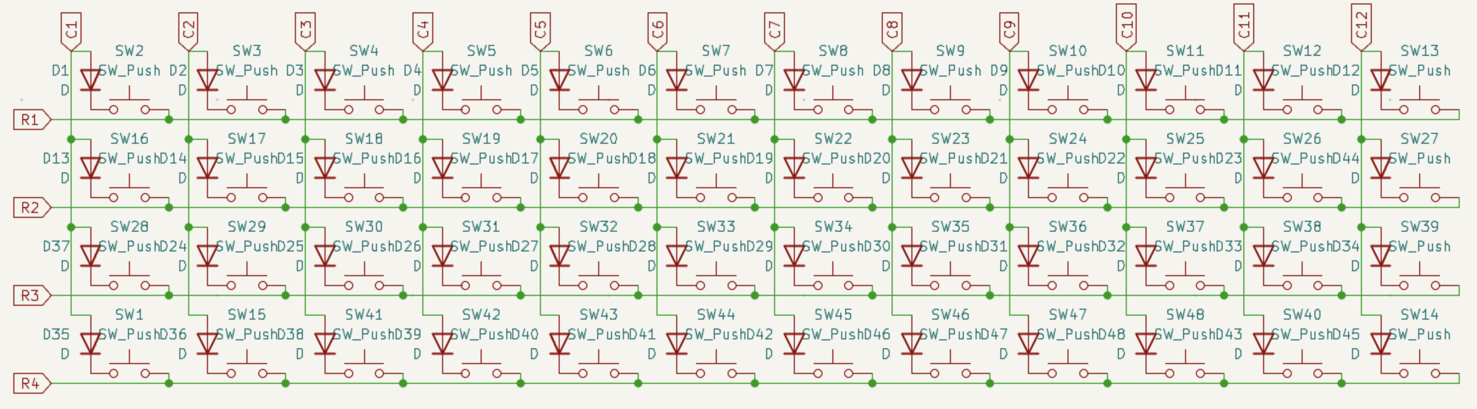
These row/columns use 16 GPIO pins on the nRF, which is most of them. However, there’s still a pin available for the charging indicator on the TP4057.

And finally, the entire schematic.